DS600 ?.5癈 Accurate Analog-Output Temperature Sensor
2 of 5
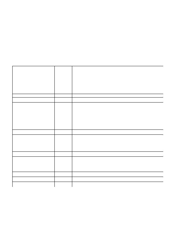
ABSOLUTE MAXIMUM RATINGS
Voltage Range on Any Pin (except CTG) Relative to Ground
-0.5V to +6.0V
Voltage Range on CTG Relative to Ground
-0.5 to +0.5V
Operating Temperature Range
-40癈 to +125癈
Storage Temperature Range
-55癈 to +125癈
Soldering Temperature (10s)
+260癈 (See IPC/JEDEC J-STD-020A)
Reflow Oven Temperature
+220癈
Stresses beyond those listed under
Absolute Maximum Ratings
may cause permanent damage to the device. These are stress ratings only,
and functional operation of the device at these or any other conditions beyond those indicated in the operational sections of the specifications is
not implied. Exposure to the absolute maximum rating conditions for extended periods may affect device reliability.
DC ELECTRICAL CHARACTERISTICS
(V
CC
= 2.7V to 5.5V, T
A
= -40癈 to +125癈.)
PARAMETER
SYMBOL
CONDITIONS
MIN
TYP
MAX
UNITS
Supply Voltage
V
DD
2.7
5.5
V
-20癈 to +100癈
?.5
Thermometer Error
T
ERR
-40癈 to +125癈
?.75
癈
Output Gain
擵/擳
6.45
mV/癈
V
OUT
DC Offset
V
OS
0癈
509
mV
Low-Level Input Voltage (SD)
V
IL
-0.5
0.3 x V
DD
V
High-Level Input Voltage (SD)
V
IH
0.7 x V
DD
V
DD
+ 0.5
V
SD Input Capacitance
C
SD
5
pF
VTH Input Capacitance
C
VTH
5
pF
Low-Level Output Voltage
(TO, TO)
V
OL
4mA sink current
0
0.4
V
Supply Current
I
DD
140
礎
Shutdown Current
I
SD
2.5
礎
Input Current (V
TH
)
I
TH
0.01
1
礎
Input Resistance (V
TH
)
R
TH
5
M&
Leakage Current (SD)
I
L
0.01
1
礎
External Load Capacitance
on V
OUT
C
EL
50
pF
V
OUT
Source Current
I
OSO
10
礎
V
OUT
Sink Current
I
OSI
10
礎
Output Impedance (V
OUT
)
R
OUT
100
&
Power-Up Time
t
POWERUP
10
ms
Nonlinearity
?.2
癈
Comparator Offset
?
mV
Comparator Response Time
t
COMP
20
ms
发布紧急采购,3分钟左右您将得到回复。
相关PDF资料
DS620U+
IC THERMOMETER/STAT DIG 8MSOP
DS7505U+T&R
IC DGTL THERMOMETER 2WIRE 8-USOP
DS75LVU+T&R
IC SENSOR TEMP DIGITAL 8MSOP
DS75LXS+
IC THERMOMETER/STAT DIG 8-SOIC
DS75U+T&R
IC THERMOMETER/STAT DIG 8-MSOP
FAN4010IL6X_F113
IC CURRENT SENSE 0.2% 6MLP
FAN5069EMTCX
IC REG DL BCK/LINEAR 16TSSOP
HIP1011BCB-T
IC CTRLR HOT PLUG PCI 16-SOIC
相关代理商/技术参数
DS601P
功能描述:烙铁 SOLDERING IRON
RoHS:否 制造商:Weller 产品:Soldering Stations 类型:Digital, Iron, Stand, Cleaner 瓦特:50 W 最大温度:+ 850 F 电缆类型:US Cord Included
DS6-02P
制造商:Cooper Bussmann 功能描述:SIDE INSERTION BRIDGE, 2 POLE, FOR DP45 - Bulk 制造商:COOPER BUSSMANN 功能描述:SIDE INSERTION BRIDGE, 2 POLE, FOR DP45
DS6-03P
制造商:Cooper Bussmann 功能描述:TOP SCREW-ON INSERTION BRIDGE, 3 POLE, F - Bulk 制造商:COOPER BUSSMANN 功能描述:TOP SCREW-ON INSERTION BRIDGE, 3 POLE, F
DS6-04P
制造商:Cooper Bussmann 功能描述:TOP SCREW-ON INSERTION BRIDGE, 4 POLE, F - Bulk 制造商:COOPER BUSSMANN 功能描述:TOP SCREW-ON INSERTION BRIDGE, 4 POLE, F
DS60-FAX
制造商:Leviton Manufacturing Co 功能描述:
DS60R
制造商:Maxim Integrated Products 功能描述:SOT23 TEMP SENSOR T&R - Tape and Reel 制造商:Maxim Integrated Products 功能描述:TEMPERATURE SENSOR SMD SOT-23-3
DS60R/T&R
制造商:Maxim Integrated Products 功能描述:SOT23 TEMP SENSOR T&R - Tape and Reel
DS60R+
制造商:Maxim Integrated Products 功能描述:TEMPERATURE SENSOR SMD SOT-23-3